Potential Divider Bias
A potential divider bias, also known as voltage divider bias, is a method used for the dc biasing of bipolar junction transistors (BJT) in a simple amplifier circuit. The circuit usually consists of biasing resistors in a voltage divider network whose values are determined through circuit analysis. Used in the field of electronic engineering, it forms an important part of small signal analysis for emitter-stabilised circuits. The dc biasing of BJTs is a complicated methodology as there is no single formula to provide the answers. It involves understanding the "Q-Point" and the "DC Load Line", as well as circuit analysis. The following article looks into biasing a simple common-emitter NPN BJT circuit employed within an amplifier.
Why bias a transistor?

A NPN BJT is a component that conducts when there is a positive voltage at the base junction. A positive voltage at the base with respect to the emitter creates a current that flows into the transistor's base junction. The transistor cannot conduct if the voltage at the base is negative because current will not flow into the transistor. Since an audio signal waveform consists of a positive half and negative half, the transistor would conduct only for the positive half and ignore the negative half thus causing clipping. One way to solve this problem is to offset the input signal by shifting it all into the positive region. A small amount of positive voltage at the base will make this shift happen and therefore bias the input signal to the positive operating range of the transistor.
Bias Circuit
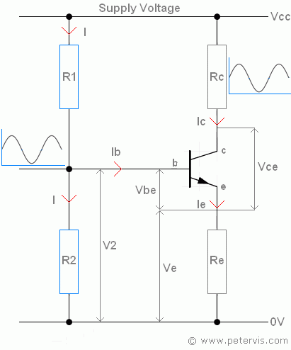
In the circuit above, R1 and R2 form a voltage divider network. This type of network has the effect of offsetting the input signal. Instead of swinging around 0 V, the signal then swings along a positive DC offset voltage. The resistors R1 and R2 determine this offset voltage.
Due to the biasing voltage at the base junction of the transistor, the transistor will always conduct slightly and consequently there will be a current Ic flowing even when there is no signal at the base. This current, known as zero-signal collector current, represents the proper offset required to push the signal into the positive half of the transistors operation. In order to calculate the values of R1 and R2 one must first find the value of Ve, Re, Ic, and the Q point, and the calculations are very simple.
Q Point
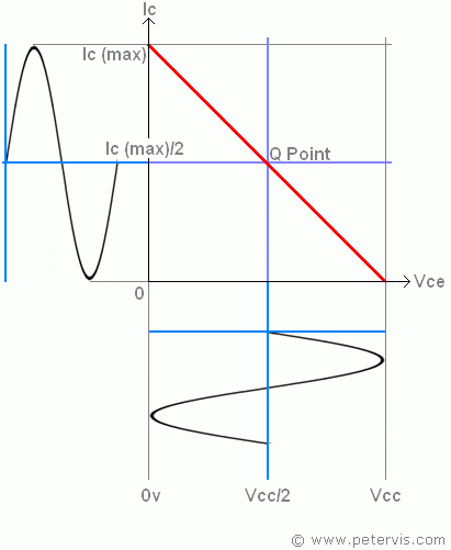
For maximum output performance, amplifiers are usually midpoint biased. This is simply Vcc / 2 where Vcc is the supply voltage to the amplifier circuit. The current is usually half of the maximum collector rating of the transistor. Therefore, if the maximum collector current were to be Ic (max) then the midpoint would be given by the following expression.
Ic (max) / 2
When the transistor operates in this Q region, the output signal swings around Vcc / 2, thus avoiding clipping. The dc load line shown in red helps to find the mid-point operation. As you can see, when the signal swings around this midpoint the negative half of the signal remains in the positive region.
Transistor Amplifier Biasing Example
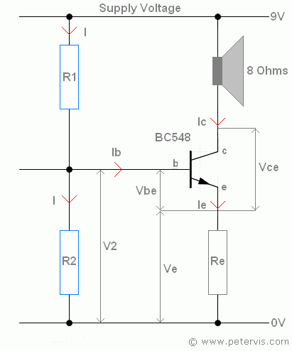
In a BJT circuit, what are the values of the voltage divider resistors for a "Class A" operation? In this circuit application, assume the supply voltage Vcc = 9 V. The load is an 8 Ω speaker, hence Rc = 8. Assume the circuit to have a BC548 transistor with the following parameters.
- Ic(max) = 500 mA
- Vbe = 0.58 V
- Gain hFE is between 110 and 800
Gain Calculation
When the manual indicates a maximum and minimum value for hFE, my old data book indicates that you should calculate the geometric average of the two values as follows.
√ (110 × 800) = 297
Therefore, a suitable value for hFE is 297.
Step 1: Find the Operating Q Point
For midpoint operation, the operating point is easy to find, and it is as follows for the collector current.
Ic(max) / 2 = Ic
500 mA / 2 = 250 mA.
The midpoint operation for the voltage Vce is as follows.
Vcc / 2 = Vce
9 / 2 = 4.5 V
Therefore, for midpoint operation, the Q Point is given by the following expression.
(Vce = 4.5 V, Ic = 0.25 A)
Step 2: Base current Ib
From your college days, you might remember the lecturer saying that hFE is the dc current gain given by Ic / Ib. Therefore, we can use the following formula.
hFE = Ic / Ib
Rearranging the above formula for the base current provides the following.
Ib = Ic / hFE
We know that the collector current for midpoint operation is 0.25, and the hFE is 297, therefore the base current Ib is 0.000842 A.
Step 3: Stability Factor and Current I
The current "I" flows through both resistors R1 and R2. Very little flows into the base of the transistor and is a negligible amount.
To ensure a good stability factor, the current "I" flowing through the resistors should be in the magnitude of 10 times the base current flow as following.
I = 10 × Ib
I = 10 × 0.000842
I = 0.00842 A
Step 4: Sum (R1 + R2)
Since we know the voltage across the voltage divider network to be Vcc, and we have a value of the current "I" flowing through the resistors, we may calculate the sum of R1 + R2 as follows.
(R1 + R2) = Vcc / I
(R1 + R2) = 9 / 0.00842
(R1 + R2) = 1069 Ω
This value will be useful to us in step 7 when calculating the individual values of the resistors.
Step 5: Find Re
All the voltages across the resistors and transistor add up to give the following expression. You will need to follow this in the diagram above.
Vcc = Ve + Vc + Vce
The following expressions for voltage are simply a product of resistance and the current flowing through them.
Ve = Ie × Re
Vc = Ic × Rc
Substitute the expressions shown above into the previous formula to give the following.
Vcc = (Ie × Re) + (Ic × Rc) + Vce
However, Ic and Ie are very similar, with a negligible difference, hence Ie can be removed from the equation and replaced by Ic to give the following expression.
Vcc = (Ic × Re) + (Ic × Rc) + Vce
We now need to transpose the above expression for Re and therefore bring the +Vce term to the LHS to give the following.
Vcc - Vce = (Ic × Re) + (Ic × Rc)
Now we divide the above expression throughout by Ic to bring this term to the LHS, because on the RHS the terms cancel out to give the following.
(Vcc - Vce) / Ic = (Re + Rc)
Finally, we subtract both sides by Rc to bring the term on the LHS to give the following expression.
((Vcc - Vce) / Ic) - Rc = Re
Vcc = 9
Vce = 4.5
Ic = 0.25
Rc = 8
Since we have the values of all the parameters within the formula, we can substitute them in to find the value of Re which is 10 Ω.
Step 6: Find V2
In this step of the circuit analysis, we need to find the voltage across resistor R2. The voltage across R2 should be equal to the sum of the voltages across Re, and Vbe. This gives us the following expression.
V2 = Ve + Vbe
From the transistor literature, we know that Vbe = 0.58 V, therefore we need to find the voltage across resistor Re. The voltage across Re is easily found because we know its resistance, which we calculated in an earlier step, and the current flowing through it.
Ve = Ic × Re
Ve = 0.25 × 10
Ve = 2.5
Therefore, we can now find the voltage V2.
V2 = 2.5 + 0.58
V2 = 3.08 V
Step 7: R2
In this step, we find the value of the resistor R2. Since we know the voltage across R2 and we know the current flowing through it, the following expression may be used.
R2 = V2 / I
R2 = 3.08 / 0.00842
R2 = 366 Ω
Step 8: R1
In step 4 we calculated that the sum of resistor R1 and resistor R2 was 1069 Ω. Since we know that R2 is 366 Ω, we can calculate the value of R1 by subtraction.
R1 = 1069 - R2
R1 = 703 Ω
Step 9: Biasing Resistor Values
Finally, we have an answer for the resistor values required for R1 and R2 potential divider bias network.
R1 = 703 Ω
R2 = 366 Ω
Transistor Bias Calculator
I have written a calculator program that does this exact same calculation, which you can follow and try with alternative transistor values. This might be useful for the university students who need to compare the figures at various stages to check their work.
Summary
If you follow the steps in sequence shown above then it should be possible to solve the resistor values for any BJT amplifier circuit. As you can see, each successive step relies on the results of the previous steps. It is like a huge mathematical jigsaw puzzle, which all comes together in the end. If you still do not understand it, then just look for any lecturer by the name of Johnson, as they tend to be the best analogue electronics teachers.
This Article Continues...
Potential DividerPotential Divider Formula Derivation
Potential Divider Bias
Potential Divider with NTC Thermistor
Potential Divider Circuit with LDR
Potential Divider Questions
Common Source Amplifier Potential Divider Bias
Ohm's Law
Resistor Symbol