PT2399 Testing and Troubleshooting

The PT2399 is a complex IC internally consisting of analogue and digital circuitry. The analogue circuits consist of the op-amps whose main pins are exposed so the user can connect capacitors and resistors to make low-pass filters. The digital circuitry consists of analogue to digital converter (ADC), digital to analogue converter (DAC), 44 Kbits RAM, and some digital computer circuitry that stores the sampled data in RAM and retrieves it again after a certain set delay.

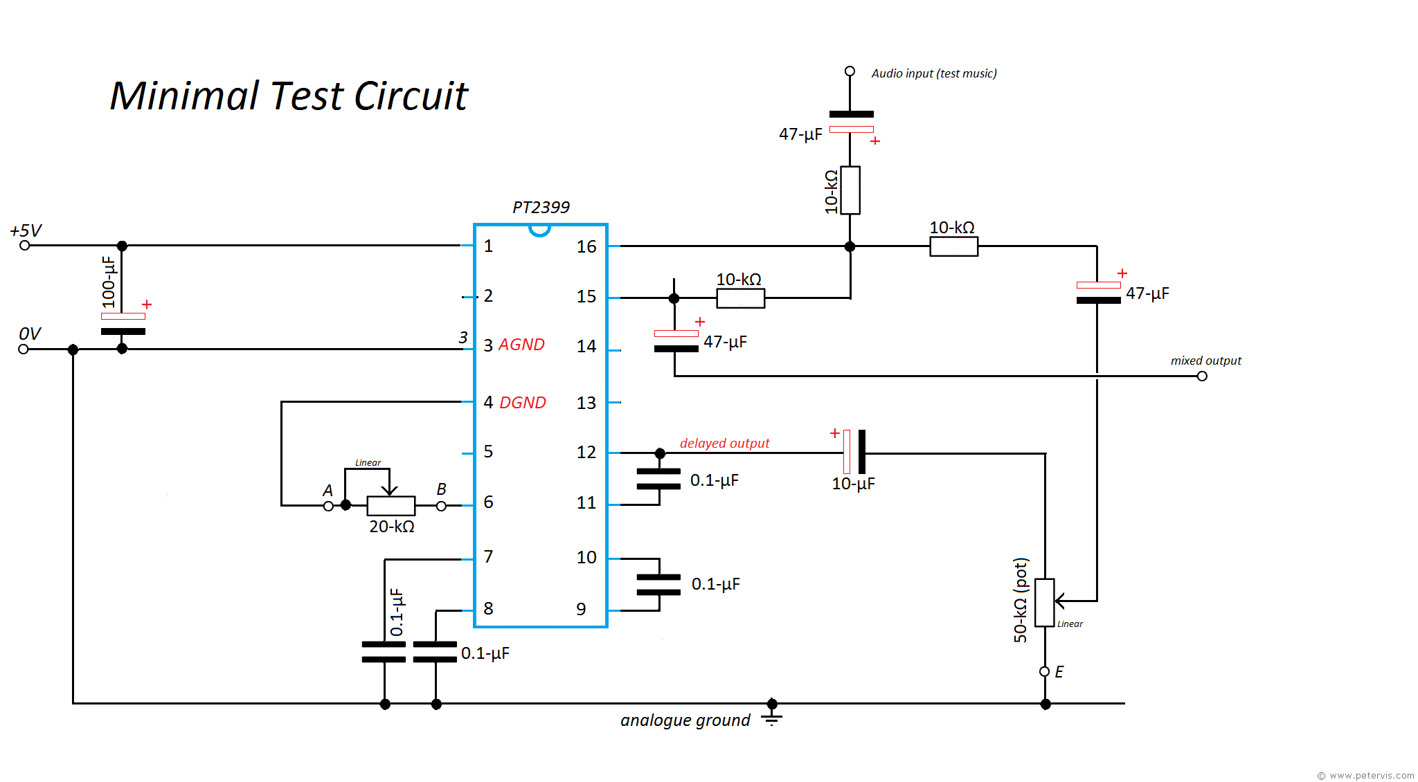
When I received the PT2399 IC, I decided to experiment with it on breadboard just to see what the pins did, and whether the IC worked at all. I did not want to build the full circuit with the LPF1 and LPF2 filters but figured that I should be able to hear the delayed sound through pins 9 and 12 if I install the 0.1 µF capacitors between pins 9 and 10, and pins 11 and 12. Hence this is the minimal circuit I made just for experimenting purposes. It turned out to be very useful as it gave me a greater insight into the workings of this IC.
For the power supply I was using the +5 V supplied by the breadboard between pin 1 and 3 (AGND). I fitted the variable resistor between pin 6 and digital ground and made sure it was at mid point. The 0.1 µF capacitors were straightforward to install so I installed all of those as well.
I used an audio probe to trace the audio as it went through the IC. This is simply a small power amplifier, fitted with headphones. Its input is connected to a probe that is decoupled with an electrolytic capacitor to block any harmful DC currents.

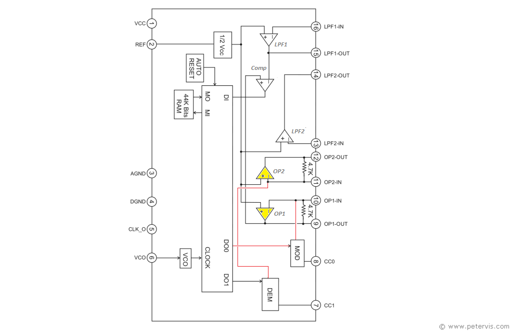
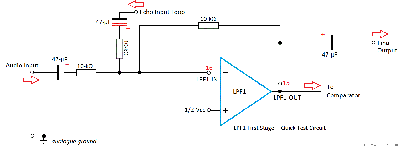
In this basic circuit, the delayed output from pin 12 goes through a DC blocking capacitor to the 50 kΩ potentiometer. The wiper output connects back to the input stage to mix with the original input signal. The only internal op-amp I used was the one for LPF1 where the input pin is on pin 16 and output in on pin 15. The output of this op-amp also internally feeds a comparator, and its output starts the whole show as it were. Hence a 10 kΩ resistor across these pins provides the op-amp feedback resistance whilst the 10 kΩ resistors at the input end provide the summing function at the virtual earth. Since the delayed output is mixed back into the first stage, we take the final output from pin 15 which went into my bench amplifier so I could hear what it sounded like. For the input signal, I simply fed an audio signal from my walkman headphone output. At first, I heard only the input signal and there was no echo. So I placed the audio probe at all the pins to see what they sounded like. Pin 5 had clock noise, which is expected as it is the clock output pin as shown in the block diagram. There was also a digital clock noise at pin 6, and some aliasing noises at pins 7 and 8.
Pin 12 where the delayed analogue output signal emerges had no signal. At pin 16, I could hear the input signal, and it was also present at pin 15, however there was no echo when adjusting all the pots. So I decided to attach the audio probe to pin 12 and decided to see what happens to the sound there if I adjusted the pots. However, there was still no audio present there. So like all IT guys, when you are out of ideas, it is always a good idea to re-boot, therefore I decided to switch OFF the power to the IC and switch it ON again, and strangely, this time there was audio coming out of pin 12. So I flicked the power switch ON-OFF again and the sound was gone!
After flicking the power switch ON/OFF multiple times I noticed that sometimes the delayed sound would be present at pin 12 and sometimes not! The variable resistor at pin 6 was set to the full 20 kΩ resistance, so I figured maybe not placing the series resistor had something to do with it. So I disconnected the variable resistor from pin 6, and then switched ON the power, and then connected the variable resistor, and the sound from pin 12 came back and echoes could be heard.
I discovered that the circuit worked more often if the pin 6 variable resistor was disconnected first, then power to the IC applied, and then the variable resistor connected. I also experimented with different resistance values at pin 6, however it had no discernable effect on the start-up. The only time it seemed to work for sure was when there was no resistance connected at pin 6. Hence, clearly, what was needed was a logic circuit that connected the ground to the variable resistor after some delay. However, I should not have to do this and the IC should work since the documentation clearly shows a table with resistance values at pin 6 going as low as 0.5 Ω. I hope that the manufacturer soon publishes full documentation together with any limitations, if indeed there are any. Therefore, I considered this a start-up bug. Whether this affects only a small batch of a version, or perhaps all the ICs is something I am going to find out after I get more ICs from China and UK for comparison.
When the internal computer is not working, only the analogue circuits remain operational, hence audio signal fed into pin 16 of op-amp LPF1 will produce an output at pin 15. However there will be no output from the modulator and demodulator, and consequently no delayed signal emerging.
When the internal computer is working, the modulator (MOD) output is internally fed to the OP1 operational amplifier at its inverting input; hence with the audio probe on the op-amps output pin 9, I was able to hear the audio quality. It sounded very metallic like the voice of a robot. This is understandable as the analogue waveform had quantization (stepped form) and needed smoothing. Hence the need for the multi-feedback low-pass filter LPF2 is very real and important.
The demodulator (DEM) feeds its output to the inverting pin of the of OP2 operational amplifier. Consequently, it is possible to hear its sound quality from pin 12, which is the output pin of the internal operational amplifier. The sound there also has quantization, hence it sounds metallic too.
Without the multi-feedback low pass filters LPF1 and LPF2, I discovered that the echo sound always had a metallic quality to it, and there was also noise from the clock oscillator present. Since the signal cycles through the loop, any noise component becomes progressively dominant; hence the filters are definitely required.
Basic Parameters
With the IC working, and +5 V fed through pin 1 and AGND (pin 3), I noticed that there was approximately +5 V potential difference also across pin 1 and DGND (pin 4) as well. This was good news because I could construct a simple delay circuit using the digital ground, whilst the timing capacitor charges through pin 1.
Other measurements taken with reference to analogue ground included 2.5 V at pin 2 (reference voltage), and 2.5 V found at pin 6.
This Article Continues...
Echo and Reverb BasicsGuitar Reverb
Basic Surround Delay Circuit
Basic Echo Circuit
PT2399 Overall Configuration
Testing and Troubleshooting
Pin 6 Hack
Pete's Guitar Reverb Circuit
Track Cuts
Board Links
Circuit Board Component Layout
Completed Board
Switch and Potentiometer Wiring
Chip Socket
Power Supply Circuit Diagram
Power Supply Board Layout
Power Supply Board Cuts and Links
Power Supply Board Completed
Enclosure Preparation
Guitar Reverb Completed Project
Connecting and Testing
